Innovative High Signal-to-Noise Optical Critical Dimension Measurement Technique for High Aspect Ratio Microstructures
2023/4/21
3D packaging technology is driving the size reduction and improved performance of electronic components through the use of high aspect ratio (HAR) microstructures such as through silicon vias (TSV) for vertical integration between layers of chip stacking. However, quality control of HAR structures has become a challenge for online process control as the number of chip stacking layers increases. The current offline measurement methods using scanning electron microscopes (SEMs) require slicing the sample and can damage the structure, unavoidably making it time-consuming and infeasible for modern advanced semiconductor fabrication.
To resolve this vital technology bottleneck, this research has developed an innovative optical measurement technique for critical dimension measurements in HAR structures, utilizing non-destructive, fast, and non-contact optical methods. The technique has a high signal-to-noise ratio, achieved by utilizing the high spatial coherence of a white light laser (supercontinuum laser) and an innovative design of the microscopic optical structure. This design significantly improves spatial resolution and lighting efficiency, thereby overcoming the limitations of existing spectral reflectometry and scatterometry techniques. Unlike these methods, which provide a limited field of view (FOV) and poor SNR, the developed optical technique can detect critical dimension information over a large area and provide high accuracy and measurement speed for HAR structures.
NTU search group led by Professor Liang-Chia Chen from Precision Metrology Laboratory (PML) & Department of Mechanical Engineering has successfully established an optical critical dimension (CD) measurement technique using effective direct and inverse modeling methods for precise CD measurement. The direct measurement method involves analyzing the measurement signal directly. The top size of the structure is measured by optical imaging, while the depth is obtained by Fourier analysis of the reflected spectral signal. Additionally, the study developed an inverse measurement method using the finite difference time domain (FDTD) method to establish the electromagnetic model of the optical system. The particle swarm optimization (PSO) is used to fit the experimental measurement signal with the electromagnetic simulation signal to reconstruct the CD parameters of multiple structures, including TCD, BCD, and depth, among other CDs. The experimental results demonstrate that with a 150x objective lens, the spot size can be controlled within 1.2 μm, enabling high spatial resolution and single microstructure CD measurement. In an example of measuring a TSV with a nominal depth of 80 μm, the SNR of depth measurement is improved by approximately 28 times compared to using an incoherent light source. Overall, the direct measurement method shows good consistency with SEM measurement values, with a deviation of less than 2.5% of SEM measurement values and a standard deviation of fewer than 20 nanometers over 30 measurements.
Read the journal article on Optics and Lasers in Engineering: https://www.sciencedirect.com/science/article/pii/S0143816623000921
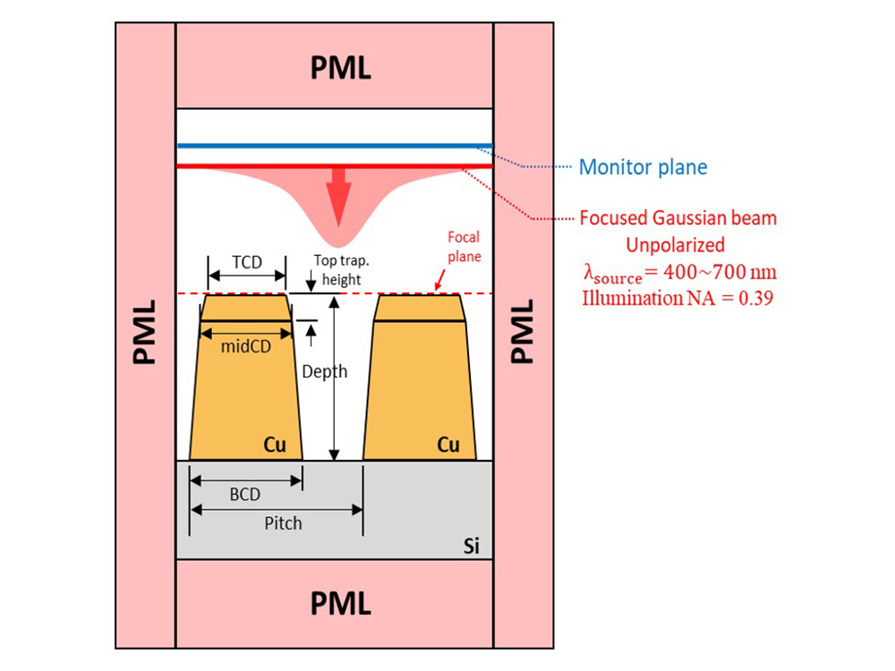
Optical simulation model framework.
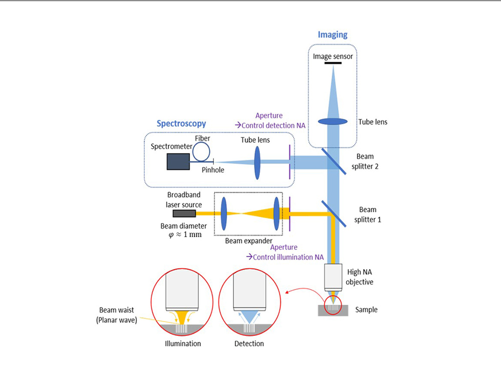
Optical system schematic diagram.
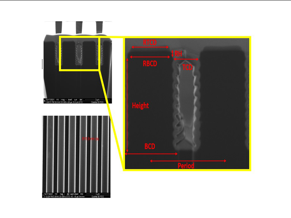
Electron microscope images of high aspect ratio structure.