Taiwan-Japan Cooperation on the Research of High‐Performance Nonvolatile Organic Photonic Transistor Memory Devices Using Conjugated Rod–Coil Materials as a Floating Gate
Prof. Wen‐Chang Chen (陳文章) of Department of Chemical Engineering, National Taiwan University has cooperated with Prof. Toshifumi Satoh (佐藤敏文) of Graduate School of Engineering, Hokkaido University for a long time, succeeding in developing high‐performance nonvolatile organic photonic transistor memory devices using conjugated rod–coil materials. The research result is published in Advanced Materials, the well-known scientific journal of materials science.
The memory device technology nowadays focuses on the miniaturization technology and three-dimensional stacking methods to meet the increasing demand for its performance and storage density. However, under the situation of complex manufacturing processes, the difficulties of development technology and high manufacturing costs gradually become a problem. Though the next-generation organic memory devices composed of organic semiconductors, on the other hand, are cheaper, lighter, and more flexible, arousing research interest in recent years, it remains issues such as operating voltage, response speed and long-term stability to be optimized.
Prof. Wen‐Chang Chen has devoted to the development of memory devices and materials for years. In 2017, he firstly proposed the concept of photonic inorganic/organic composite floating gate, developing a memory device using light as the switch, controllable for different wavelengths with multiple-bit storage characteristics (Advanced Materials, 2017, vol.29, page 1701645).
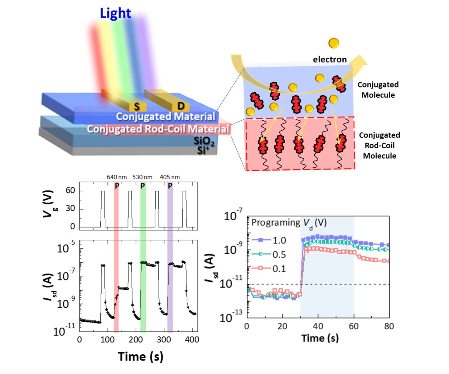
Prof. Wen‐Chang Chen and Prof. Toshifumi Satoh have cooperated for many years on the development of nanomaterials and discovered a new approach using conjugated rod–coil materials as a floating gate in the fabrication of nonvolatile photonic transistor memory devices, consisting of n‐type Sol‐PDI and p‐type C10‐DNTT. Sol‐PDI and C10‐DNTT are used as dual functions of charge‐trapping (conjugated rod) and tunneling (insulating coil), while n‐type BPE‐PDI and p‐type DNTT are employed as the corresponding transporting layers. By using the same conjugated rod in the memory layer and transporting channel with a self‐assembled structure, both n‐type and p‐type memory devices exhibit a fast response, a high current contrast between “Photo‐On” and “Electrical‐Off” bistable states over 105, and an extremely low programing driving force of 0.1 V. The fabricated photon‐driven memory devices exhibit a quick response to different wavelengths of light and a broadband light response that highlight their promising potential for light‐recorder and synaptic device applications. (as shown in the figure below) 。
This research result is a breakthrough for the development of the material design and response mechanism of the next-generation organic photon‐driven components. Other than the publication in journal Advanced Materials on Sep. 10th, 2020 (Advanced Materials, 2020, vol. 32, Page 2002638), this press release is also issued simultaneously with Hokkaido University.